Introduction
In the article Processors – Part 1, the most basic concepts of a processor were discussed, such as clock, Front Side Bus (FSB) and cache memory. In this second part, you will learn about other concepts related to processors, such as miniaturization are taking and encapsulation. However, the most important thing is that you you will also find the answer to a very common question: as the processors are manufactured?
It is clear that this is a subject of extreme complexity. By this reason, only the most basic concepts will be explained here. However, this explanation will be sufficient to you can have an idea of how the processors are manufactured. Before you start, a tip: read the first part of this article for not if you “lose” in the face of any technical term mentioned here ;).
We’re going there?
Silicon
The first step in the manufacture of processors is obviously, in obtaining raw materials. Generally,the chips are formed of silicon, and with the processors this is no different. The silicon is a chemical element extremely abundant, so much so that it is considered the second most common on Earth. It is possible to extract it from sand, granite, clay, etc.
This chemical element is used for the constitution multiple-resistant materials, such as glass and ceramics. In however, it is also a semiconductor, that is, has the ability to conduct electricity. This characteristic combined with its existence in abundance causes the silicon to be an element extremely used by the electronics industry.
To give you an idea of the importance of this material, the concentration companies that use silicon in their electronic products in several cities of California, in the USA, made with the the region received the name of Silicon Valley (Silicon Valley). It is there that are located, for example, the headquarters of AMD and Intel, the largest manufacturers of microprocessors in the world.
The manufacturing of processors
The manufacturing of the processors begins in modern centers specialized technological. These places are so the sophisticated construction of the value so high, there are few in the world. In the laboratories of these centers, a a certain amount of a crystal of silicon is placed in a sort of rod and, subsequently, embedded in the silicon cast subjected to a pressure and a temperature, extremely high – around 300. The rod is then withdrawn and rotated at the same time. This process (called technical Czochralski) it makes the material that is joined to the shank to form a sort cylinder (also known as “ingot”). Your diameter varies in accordance with the advancement of technology, but in general it has between 200 and 300 millimeters. The same goes for the length: 1 to 2 metres. It is important to note that these cylinders need to be formed of pure silicon. The process purification of this material is complex, which increases the costs of even more manufacturing.
Once you complete this step, the cylinder is “sliced”, this is cut into several parts. Each one of these divisions gets its name from the wafer. Each “slice” is polished to be perfect, without variations, spots, differences brightness or any irregularity in its composition. Its thickness generally is less than 1 mm. In a step further, each wafer will be divided into several “squares” (or “inserts”), which will later be separated and will make the processors itself.
In the next step, the surface of the wafer undergoes a process oxidation, where the application of gas – especially – oxygen and high temperature form a layer of dioxide silicon. This layer will serve as the basis for the construction thousands and thousands of transistors, in a few words, tiny components able to “amplify” or “switch” signals electrical, in addition to other related functions.
In the next step, the wafers go through a process where they receive a layer of material is photosensitive, that is, one that reacts in the light. In this step, each of the blocks which will in processor receives ultraviolet light at certain points and in certain intensities. The points of the layer of photosensitive they react to the ultraviolet light become more “gelatinous” and are subsequently removed, leaving exposed the corresponding points of the layer of dioxide silicon. With this, the points covered with a layer of photosensitive and dots covered with silicon dioxide. Obviously, the layer the photosensitive remaining is silicon dioxide for cheap. The parts of the latter that are not protected by layer photosensitive are then removed through of another procedure. In the next step, the layer of photosensitive is removed. What is left over is then used as a structure for the mounting of the transistors, a procedure that continues being made from the application of more materials and exposure to ultraviolet light.
Those who have some experience with photo-based movies, probably you will notice that the steps outlined above remember a lot of the procedures photo development. In fact, the principles are essentially the same.
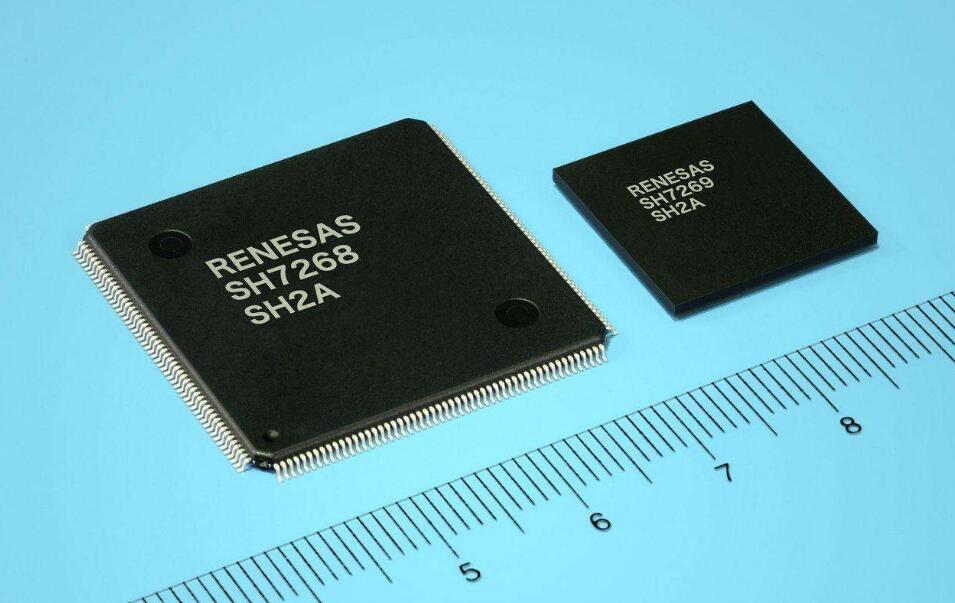
It is important to note that a single processor can contain millions of transistors. Just as an example, the first the processors of the line Intel Core 2 Duo they have about 291 million transistors into a single chip. As is the case with any processor, these transistors are divided and organized into groups, where each group is responsible by a function.
Once you have finished the mounting of the transistors, the wafers are “cut” in a format reminiscent of small squares or lozenges. Each unit if you transform into a processor. As the wafers are round,what is left of the edge, obviously, can’t turn a processor, then this material is discarded, as well as any unit that display defect or abnormality.
You might have asked themselves whether it would not be ideal to manufacture wafers square or rectangular to avoid waste on the edge. Theoretically, it would be, but the wafers are formed by cylinders because of the manufacturing technique explained at the beginning in this topic, where a rod is inserted in the silicon and, then, withdrawn and rotated. This procedure causes a cylinder is formed naturally.
It is important to stress that each wafer gives rise to the hundreds processors, therefore, the entire manufacturing process is carried out based on a series of care. To begin with, the laboratories of the factories are local extremely clean and protected (known as “clean room”), both is that the few people who accompany the production use clothes that resemble astronauts (as shown in the second photo of this topic). In addition, the machines responsible for the production need to be perfectly adjusted to follow the instructions of the projects of the chips that are being manufactured.
Difference of clock
When the processors get to market, they are classified in lines, for example, Intel Core 2 Duo, AMD Phenom II, and so on. Each of these lines is constituted by processors various processing speeds. As an example, the line Intel Core 2 Duo has the templates E8400, E8500 and E8600. What differentiates them is that the clock of the first is 3 GHz, the clock of the second is 3.16 GHz and, finally, the clock of the third is 3.33 GHz.
All of these processors are from the same project, therefore, they have the same architecture. What makes a model more quickly the other is that the manufacturing of the fastest was more perfect than the models immediately below. Small details during the entire manufacturing process for make, within of a the same wafer, the “pads” are slightly different one of the other. This can happen, for example, because of small deviations in the layers, small differences in the passage of the beam of light, etc.
For this reason, the wafers undergo tests that indicate with which frequency each chip can use. Only after this, the wafer is cut and the chips pass to the stage of encapsulation. These tests also point out which chips should be discarded for not they have conditions of use.
Miniaturization are taking
The industry managed to raise the capacity of the processors to the over time without, for both, had to increase the physical size of these devices. This is possible thanks to nanotechnology, in a nutshell, a branch of science that involves the research that deal with items measured in the house of nanometers. For those who don’t know, a nanometer is equivalent to one millionth mm, that is, a millimeter divided by a million, and its abbreviation is nm. The most widely used measure, however,is the micron, which is equivalent to a thousandth of a millimeter that is, a millimeter divided by one thousand.
Thanks to the research of nanotechnology, it is possible to leave the transistors of chips are becoming smaller and smaller. The processor The Intel 486, for example, has about 1 million transistors, being that each one has nearly 1 micron in size. Very small, doesn’t it? In fact, it is a size that is monstrous, compared to the processors current. Just to give you an idea, in this article has been said that the first processors of the line Intel Core 2 Duo come with about 291 million transistors. These chips use technology for the manufacture of 0,065 micron (or 65 nanometer), the most recent in this line are manufactured with 0,045 micron (45-nanometer).
The research on miniaturization are taking chips indicate that it will be possible to take this process to the house of the 25 nanometers (or a value not much smaller than this). After addition, the industry will reach a physical limit where the transistors are likely to be formed by a few atoms and can no longer be decremented. It is clear that searches are already in progress for create an output for this problem. One of them is the “computing quantum” , that much more than work around the physical limits of the processors of the computing classical”, may revolutionize computing as a whole.
Encapsulation of processors
In the steps of the tunnel, the processor is inserted into a kind of a “frame” which protects and contains metal contacts for communication with the components of the computer. Each model of processor, you can count on types of different encapsulation, which vary according to your project.In general, the processors have in their upper part a kind “cover” metal called “Integrated HeatSpreader”(IHS), which serves to protect it and, many times, to facilitate the dissipation of heat. This component normally covers the entire top of the chip and, inside it, in the centre, is the the processor itself (also called “die”). In however, in some models, the IHS is not used. These cases, the absence of this protection can facilitate dispersion of heat due to direct contact of the die with the cpu cooler (fan) processor and reduce manufacturing costs.
It is important to note that there are several technologies used the encapsulation of the processors. The application of each a varies according to the design of the chip. Here are the main types, having as the basis of technologies of Intel:
– PGA: abbreviation for Pin Grid Array (something like “array pin”), this is a type of encapsulation that causes the processor use contact pins that must be inserted into a fitting proper on the motherboard of the computer (see the socket, just below). Your basic material can be ceramic (Ceramic Pin Grid Array – CPGA) or plastic (Plastic Pin Grid Array – PPGA). There is also a type called Flip Chip Pin Grid Array (FC-PGA), where the insert is partially exposed in the upper part of the chip;
– SECC: acronym for Single Edge Contact Cartridge, this type causes the processor to use a plug-in linear (slightly similar to the memory slots, for example) rather contacts in the form of pins. For this, the processor is mounted within a kind of the cartridge;
– SEPP: acronym for Single Edge Processor Package, this type is similar to the SECC, however, the processor is coupled on a board that is not protected by a cartridge;
– LGA: acronym for Land Grid Array this is a standard recent from Intel. Has some similarity with the standards of the PGA, having as main difference the fact that the processors do not use contact pins on its bottom, but rather points of metal. When the processor is embedded on the motherboard, these points are in contact with pins on the existing socket (remembering that in the standards PGA there are holes instead of pins in the socket). With regard to the LGA, Intel used (up to the closing of this text in the AbbreviationFinder) a type called FC-LGA4 (Flip Chip Land Grid Array, where the number 4 indicates the revision number of the standard).
In the lower part of the processors with tunnels in the standards PGA and the like, are exposed to a series of metal contacts that make the communication between the processor itself and the components of the computer. For this, the contacts are recessed in an area proper on the motherboard of the machine, the call socket (or socket). It happens that the amount and the disposition these pins varies depending on the model of the processor. For example, the line Intel Core 2 Duo, and some of the more recent models of the line Pentium 4 use the socket 775 (LGA 775):
This makes it clear that it is necessary to use the motherboard and processor with the same socket at the time of assembling a computer. However, it is important to stress that this is not warranty of compatibility between the two. It is possible, for example, that a particular motherboard use the same socket a processor released after her arrival to the market. Despite both have the same socket, a mismatch may occur, as that is the chipset of the motherboard may not have been prepared to receive one processor. For this reason, it is important to check always on the manufacturer’s website or in the manual of the motherboard which processors it supports.
Note that the arrangement of pins (or points of contact, in the case of chips with encapsulation type LGA) is the user has only one way to fit the processor on the motherboard. With this, to prevent wrong entries that may result in damage to the computer. For this reason, if the user is not able to fit in to the processor, you should avoid efforts and look in the manual of the motherboard the the correct orientation.
Names-code of the cores
Every processor comes to the market with a name that allows you to easily identify you, such as Pentium 4, Core 2 Duo, Itanium, Athlon, 64, Phenom, etc. What few people know is that the core of the processors receive another denomination even before its release official: the name-code.
The use of the names-code is important because it allows to distinguish the characteristics of architecture each chip. Even within a given row is it possible find processors with differences in your project. We can use as example the first models of the line Intel Core 2 Duo, that are based in the core name Conroe and Merom. The the first is targeted at desktops, while the second is oriented portable computers (such as notebooks). Thus, the Merom has features that optimize its performance to require less energy (for example, use voltage lower and FSB reduced, if compared to the Conroe).
Ending
The processors are devices highly complex, but also fascinating. I find it hard to believe that a chip that fits at the tip of the finger can accomplish so many things. Unfortunately, it is not it is possible to find many documents and images that detail the locations and the stages of the manufacturing of the processors. And it is not difficult to understand the reason: these places are quite protected and come with a policy that is extremely strict access, as a simple grain of dust or even the lights flash from cameras can damage the production. In addition, it is known that each manufacturer tries to protect yourself from industrial espionage.